Semiconductor device fabrication: Difference between revisions
CSV import Tags: mobile edit mobile web edit |
CSV import |
||
| Line 47: | Line 47: | ||
{{Electronics-stub}} | {{Electronics-stub}} | ||
==Semiconductor_device_fabrication== | |||
<gallery> | |||
File:Wafertraksystem.jpg|Wafer track system | |||
File:1957(Figure_9)-Gate_oxide_transistor_by_Frosch_and_Derrick.png|Gate oxide transistor by Frosch and Derrick | |||
File:Intel_Fab_12,_Fab_22,_Fab_32.jpg|Intel Fab 12, Fab 22, Fab 32 | |||
File:Semiconductor_photomask.jpg|Semiconductor photomask | |||
File:Comparison_semiconductor_process_nodes.svg|Comparison semiconductor process nodes | |||
File:Siliconchip_by_shapeshifter.png|Silicon chip by shapeshifter | |||
</gallery> | |||
Latest revision as of 20:51, 25 February 2025
Semiconductor device fabrication is the process used to create the integrated circuits that are present in everyday electrical and electronic devices. It is a multiple-step sequence of photolithographic and chemical processing steps during which electronic circuits are gradually created on a wafer made of pure semiconducting material. Silicon is the most commonly used semiconductor material today, not only because it is readily available, but also because it has a very favorable quality that allows for the creation of both N-type and P-type transistors.
Overview[edit]
The process of semiconductor device fabrication involves a combination of photolithography, etching, chemical vapor deposition (CVD), physical vapor deposition (PVD), ion implantation, and other processes. Each of these steps is critical for the proper functioning of the finished semiconductor device. The entire process is performed in highly specialized facilities known as semiconductor fabrication plants or fabs.
Key Processes[edit]
Photolithography[edit]
Photolithography is a process used to transfer patterns onto the semiconductor wafer. This is achieved by exposing a photosensitive material to ultraviolet light through a mask, which selectively hardens the material where the circuit should be created.
Etching[edit]
Etching is the process of removing selected areas of the semiconductor material or its layers. It can be done through wet chemical processes or dry processes like plasma etching.
Chemical Vapor Deposition (CVD)[edit]
CVD is used to deposit thin films of various materials onto the semiconductor wafer. These materials could be conductive, insulative, or semiconductive. The process involves a chemical reaction occurring in the vapor phase, which deposits the desired material onto the wafer.
Physical Vapor Deposition (PVD)[edit]
PVD involves the physical transfer of material from a source to the wafer surface. Techniques such as sputtering or evaporation are used to deposit layers of materials onto the wafer.
Ion Implantation[edit]
Ion implantation is a process used to introduce impurities into the semiconductor wafer. These impurities, known as dopants, are necessary to modify the electrical properties of the semiconductor material, allowing for the creation of N-type and P-type regions.
Fabrication Steps[edit]
The fabrication of a semiconductor device involves numerous steps, each carefully controlled to ensure the integrity of the previous steps and the overall functionality of the final product. These steps include:
1. Wafer Preparation: The process begins with the preparation of the semiconductor wafer, which is typically made of silicon.
2. Oxidation: A layer of silicon dioxide is grown or deposited on the wafer to serve as an insulator.
3. Photolithography: This step involves transferring the circuit pattern onto the wafer.
4. Etching: The unwanted silicon dioxide is removed, exposing the silicon in areas where transistors are to be created.
5. Doping: Impurities are introduced into the exposed areas to create N-type or P-type regions.
6. Metallization: Metal contacts are created to allow for electrical connectivity between the semiconductor device and the outside world.
7. Assembly and Packaging: The completed semiconductor devices are assembled into packages that protect them and provide connections to other electronic components.
Challenges and Innovations[edit]
The semiconductor device fabrication process is constantly evolving to meet the demands for smaller, faster, and more energy-efficient devices. Innovations such as extreme ultraviolet lithography (EUV), FinFET transistors, and 3D semiconductor structures are at the forefront of this evolution.
Conclusion[edit]
Semiconductor device fabrication is a complex and critical process in the production of electronic devices. It involves a series of sophisticated steps that must be precisely controlled to ensure the functionality and reliability of the final product. As technology advances, the fabrication process continues to evolve, enabling the development of increasingly sophisticated electronic devices.

Semiconductor_device_fabrication[edit]
-
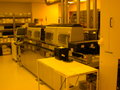 Wafer track system
 -
 Gate oxide transistor by Frosch and Derrick
 -
 Intel Fab 12, Fab 22, Fab 32
 -
 Semiconductor photomask
 -
 Comparison semiconductor process nodes
 -
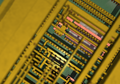 Silicon chip by shapeshifter

-Gate_oxide_transistor_by_Frosch_and_Derrick.png)


